Table of Contents
Diode Logic
The diode logic uses diodes and resistors to implement Boolean functions. Diodes function as a switch that conducts only during the forward biasing condition. The simplicity in the circuits is the main advantage of diode logic but it lacks amplification of the input signal. This limits the application of diode logic. The diode logic can implement only logic OR and logic AND operations that are non-inverting. All other logic operations cannot be implemented using diode logic. The diodes and resistors are either connected in parallel or series that function as electronic switches controlled by input logical variables. When the diode is forward biased the switch is closed and when the diode is reverse biased the switch is open.
Diode Logic (DL) OR Gate:
The diode OR gate has two inputs and an output. The output is high only if at least one input is high and is low when both the inputs are low. The circuit for a basic DL OR is shown in figure below. The OR logic gate is implemented in the diode logic by connecting the diodes parallel. The diodes are normally open switches. It is clear from the circuit that the input is applied to the anode of the diode and the output is taken at the cathode of the diode across the resistor R1 to the ground. The +5 volts always represent logic 1 or ON, and ground, or zero volts a logic 0 is represented as in figure below.
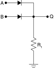
- Inputs at logic 1: In the circuit, if both the inputs are connected to +5 V or logic high input logical 1 then the diodes are forward biased and are closed. The current passes across the diode and causes high voltage drop across the resistor R1. The output is at high or logic 1. If one input is high and the other input is low, then the diode connected to the high input acts as closed switch and the output is still high.
- Inputs at logic 0: When both the inputs are connected to zero volts or ground, then the inputs are at logic 0. Both the diodes are reverse biased and switches are open and do not conduct. Therefore, the output across the resistor will also be zero volts.
Thus, the diode logic implements the OR functions. Assume that the diode induces error in the circuit. The silicon diode introduces a voltage drop of 0.65 V–0.7 V therefore even when the voltage is not exactly +5 V but +4.35 V at the output still the diodes are said to be conducting. We consider the noise margin in this case. Thus, any voltage above +3.5 volts is considered to be logic 1, any voltage below +1.5 volts shall be logic 0. Output voltages between +1.5 and +3.5 volts fall under the undefined voltage region.
DL AND Gate:
The Diode Logic (DL)-AND gate is implemented by connecting open switches in series. Since diodes are two terminal devices, they cannot be driven by grounded input voltage sources when connected in series. Thus to overcome this problem, the diodes are connected in parallel as in the case of OR diode gates with modification. To obtain AND logic instead of OR function the input and output logical variables are inverted or reversed. The circuit of DL AND gate is shown in figure below. In a diode AND gate, if both the input voltages are high then the output voltage is high. If both the inputs are low and one is low then the output voltage is low.
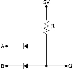
Consider the circuit for AND logic gate, the input to the diodes is connected in opposite direction. The input voltage flows across the resistor thus creating the current to flow across the anode of the diodes and then to its cathode. The output is taken across the resistor R and ground terminal. This gives the complementary voltage drop.
- Inputs at logic 1: When both the inputs A and B are at high, then the diodes are neutralized. There is no voltage drop across the diodes and the diode switches are open. Since no current flows across the resistor and no voltage drop, the output is high. Thus, the operation of diode logic AND is the reverse of diode logic OR gate since the diodes are reversed.
- Inputs at logic 0: When both the inputs are at low, the biasing voltage (+5 V) flows through the resistor and reaches the diodes and finally the input source. This causes the diodes to be forward biased and the diode switch is closed. Thus, the output voltage drop across the diode is logic 0. If one of the inputs is high and the other is maintained at low, then the diode connected to high input voltages or logic 1 is reverse biased and its input voltage is disconnected from the output. The output is again 0. Thus, this circuit performs the logical AND functions.
Disadvantages of Diode Logic
- Diode logic only permits the OR and AND functions.
- Diode logic suffers from voltage drop from one stage to the next. Unlike the active logic gates that can be integrated to larger components, the diode logic cannot be cascaded as they face few problems.
- – The diodes possess a voltage drop of 0.65 V during the forward bias condition. When the identical diodes are cascaded, this voltage is either added to or subtracted from the input of every gate. Thus, this voltage accumulates at each stage. For an OR gate, the voltage drop decreases the high voltage level (logic 1) while in an AND gate, it increases the low voltage level (logic 0).
- – The second problem the diodes face during cascading is that of the voltage divider. The input voltage sources possess an internal resistance that joins the gate resistor to produce a voltage divider action on the voltage levels. The source resistance decreases logic 1 level in an OR gate. In an AND gate, the gate resistance increases logic 0 level.
- Diode logic is used extensively to produce simple logic functions but not in integrated circuits.
- These issues restrict the usage of diode logic and have made them obsolete.
Related Post: