Table of Contents
Flip Flop
Flip-flop is a sequential logical circuit, which is an edge trigger or sensitive. The flip-flop and latch are made via different logic gates. Flip-flop is different from latch because the clock feature is not present in latches, which is important for Flip-flop operations. The output of Flip-flops will change either at the increasing edge or decreasing edge of the clock pulse, whereas the output is a change in the latch at the change of the level of clock pulse either high or low level.
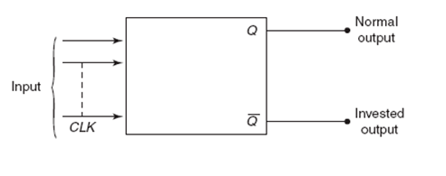
The block diagram of a standard flip-flop is shown below

A sequential circuit that has only two states, 1 or 0, is called a flip-flop. Its two outputs are complementary to each other.
Types of Flip-flops
Basically flip-flops are 4 types. These are-
- S-R FF
- D FF
- J-K FF
- T FF
Set-Reset or S-R FF:
The name of this flip-flop derives its name from set and reset states. They are also known as preset and clear states.
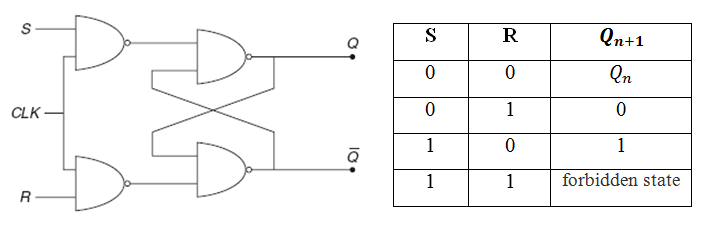
- The S-R FF is a first and basic FF, which has two inputs – S and R.
- S stands for “Set” and R stands for “Reset”.
- The input of FF is called SET if its output Q has a high value or ‘1’ state, and when it is called RESET, if output Q has a low value or ‘0’ state.
- Both the outputs are the complement of each other (i.e., output Q′ and Q ). Its output depends on the present as well as the previously stored output.
- The characteristic equation is Q_{n+1}=S+\bar{R}.Q_{n}.
- The internal circuit and the excitation table of the S-R FF is shown below
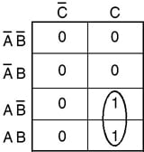
Input Conditions
- S =R= 0 is the normal resting or no change condition of the FF. In this condition, the output ports (Q and Q’) hold the previous states, either 0 or 1.
- S = 0 and R = 1 is the resets or clears state of the FF. It is because RESET has a high or ‘1’ state.
- S =1 and R =0 is the set state of the FF. It is because SET has a high or ‘1’ state.
- S = R = 1 is forbidden state of the FF. It is because both the input has a high or ‘1’ state at the same time.
Delay or D-FF:
The letter D in the D flip-flop stands for “data” as this flip-flop stores single bit temporarily.
- The S-R Flip Flop is a forbidden state. To remove this condition from the FF, connect the input terminal of S–R flip-flop with each other via an inverter or NOT gate.
- The internal structure of D FF is shown below. The inverter or NOT gate placed for ensuring that inputs S and R will never equal.
- The structure of D-FF is the same as S-R FF except for a single input terminal.
- There are D stands for ‘Delay” because the inverter produces a small delay between both the input of FF that is directly shown in outputs.
- The characteristic equation is Qn+1 = D

J-K FF:
The JK flip-flop is the most versatile of the basic flip-flops. The input of a JK flip-flop has two inputs that are traditionally labelled as J and K with no other significance to JK except being consecutive alphabets.
- The forbidden state output of S-R FF is removed in D FF, by joining both the inputs via an inverter or NOT gate. But the D FF has a single input terminal.
- The J-K FF is similar to S-R FF because it has 2 inputs i.e., J and K.
- The characteristic equation is Q_{n+1}=J.\bar{Q_{n}}+\bar{K}.Q_{n}
- Both the inputs of J-K FF are high or ‘1’, the output toggles and the forbidden or ambiguous state are removed.

Toggle or T-FF:
T flip-flop also known as trigger/toggle flip-flop is the fourth type of flip-flop. It can be constructed from SR, D, and JK flip-flops.
- The two input terminal of J-K flip-flop is connected to each other a new flip-flop is formed, which is called T Flip-flop.
- T stands for “Toggle”.
- The input of T flip-flop is high or ‘1’, the output toggles. This condition is called a toggle mode.
- The input of T flip-flop is low or ‘0’, the output hold. This condition is called hold mode.
- The characteristic equation is Q_{n+1}=T.\bar{Q_{n}}+Q_{n}.\bar{K}

Excitation Table
It shows the inputs of flip-flops when the next state and present state are known.
In the design process, generally the values of transition from the present state to the next state are known and the inputs conditions are unknown. To find the input conditions with the help of these required transition values. There is a requirement of a table that gives a relation between inputs of flip-flop and its present and next state. Such a list is called an excitation table.

Excitation Table
The Race-around Condition in flip-flops
The SR flip flop does not allow both the inputs to be HIGH. This complexity in an SR flip flop is eliminated in a JK flip flop. The inputs of a SR flip flop does not change during a clock pulse but this is not true for JK flip flop as it uses the feedback mechanism. When the outputs are given back into the inputs of the gate then this known as feedback mechanism.
Consider the JK flip flop whose inputs J = K = 1 and the output of the previous sate Q = 0. After a clock pulse of duration tp equal to propagation delay of NAND gates, the output will change to Q=1. Now, we have J=1, K=1 and Q=1. If duration of clock pulse (T) is greater than propagation delay, tp after another time interval of tp the output will change back to Q=0, hence, the output will oscillate back and forth between 0 and 1. The output is uncertain at the end of clock pulse if flip flop is level trigger. This situation is called race-around condition.
The race-around condition can be avoided if clock pulse is reduce than propagation delay of flip-flop t< tp<T, but his is not practically feasible. A more practical method for this is the use of the master-slave flip-flop.

Master-Slave JK Flip-Flop
The principle behind the master–slave JK flip-flop is similar to a master–slave D flip-flop. There can be master–slave flip-flops in all three types of flip-flops, SR, JK, and D. A Master-Slave JK flip-flop is obtained by cascading two flip-flops; the first is called the master and second is called the slave. The slave follows the master operation. The only difference being the clock signals given to master and clock that determine the output. The clock is connected to the slave through an inverter. The block diagram is shown as in figure below.

During the leading edge of the clock pulse, the data inputs are transferred to Q_{m} and \bar{Q_{m}} of the master. This state remains as long as the clock pulse is 0 at the slave. When the clock pulse goes negative on trailing edge the master becomes positive at the clock input of the slave and Q_{m} and \bar{Q_{m}} of the master flip data inputs are transferred to Q and \bar{Q} . This racing condition is averted as feedback from outputs that occurs for pulse at 0. Nevertheless it is to be noted that JK inputs should not be changed for the pulse duration which is overcome in master–slave flip-flop with data lock.
Applications of Flip-Flops
Flip-flops are used in a variety of application circuits, like the frequency division, counting circuits and data storage and transfer circuits. Some of the common uses of flip-flops are as:
- Registers
- Counters
- Memory
- Latch
Some other applications of flip flop
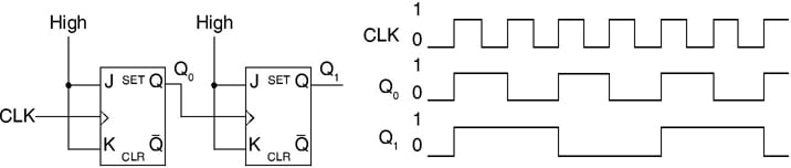
Frequency Division
When a pulse waveform is given to the clock input of a T flip-flop formed from JK flip-flop, the Q output is in the form of a square wave. The frequency of the square wave is half of the input clock frequency. The division of the clock frequency depends on the number of flip-flops instituted in the circuit. Further divisions can be achieved by increasing the flip-flops. The circuit and waveform is shown in figure below.
Parallel Data Storage
Digital systems store data in groups of bits that represent numbers, codes, or other information. These bits of data available on parallel lines are stored in the flip-flops. This operation is shown below. Each of the three parallel data lines is connected to the D input of a flip-flop. All the clock inputs are connected to a single clock, this makes the data on the D input to get stored simultaneously by the flip-flops for the positive edge of the clock.

Multivibrators
Multivibrators are used in storage of binary numbers; to count clock pulses, to perform arithmetic operations but the main application being non sinusoidal wave generation. It generates rectangular, square, sawtooth waves, etc. Multivibrators are of different types:
- Bistable multivibrator
- Monostable multivibrator
- Astable multivibrator
You may also like in hindi click here