Registers or shift registers are binary storage elements that consist of flip-flops and gates. They belong to the family of sequential circuits. The registers are referred to as clocked sequential circuits when the combinational circuits are absent. Registers are used to load and store binary information when the clock pulse of the flip-flop circuit is enabled.
The flip-flops in a register can either be JK or D flip-flops. The number of flip-flops used in a register depends on the bits to be stored. If two bits are to be stored then two flip-flops are used. Thus, each flip-flop is capable of storing only a single bit. Though the flip-flop stores the data, it is the logic gate that determines the manner in which the data is transferred into the register.
Table of Contents
Shift Register
A register capable of shifting its binary information either from right to left or left to right is called a shift register. A shift register consists of an array of flip-flops connected in cascade.
A shift register is a digital device used for storage and transfer of data. The data to be stored could be the data appearing at the output of the flip-flop. The basic building block in the shift register is the flip-flop, mainly a D-type flip-flop. Although in many of the commercial shift register ICs their internal circuit diagram might indicate the use of R-S flip-flops, a careful examination will reveal that these R-S flip-flops have been wired as D flip-flops only.
Classifications of Shift Registers
Shift registers are classified under four types, namely:
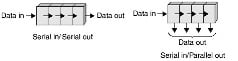
Serial In/Serial Out (SISO): One bit of data can be moved in and out of the register serially at a time.
Serial In/Parallel Out (SIPO): One bit of data can be loaded serially but the stored data can be taken out of the register parallelly.
Parallel In/Serial Out (PISO): The data can be loaded simultaneously but can be removed only as one bit at a time for each clock pulse.
Parallel In/Parallel Out (PIPO): The data can be loaded and read out into the register simultaneously. There is also a bidirectional shift register of this type where the inputs can be shifted right to left or left to right.

Serial In/Serial Out (SISO):
This type of shift register loads the data and shifts it from left to right if it is unidirectional and in both directions if it is bidirectional register. The least significant bit of the binary number is stored in the left most flip-flop and keeps shifting to get the final output at the right most flip-flop.
A 4-stage shift register using JK flip-flop is shown in figure below. The bit is loaded at the flip-flop A and output are obtained at flip-flop D after a delay of 4 clock pulses. The NAND gate connected at the input performs the gating function. The input at A is passed to the flip-flops when B = 0 and is inhibited when B = 1.

The operation of a 4-stage register shifting data 1010 from left to right is shown in figure below.

Serial In/Parallel Out (SIPO) Shift Register:
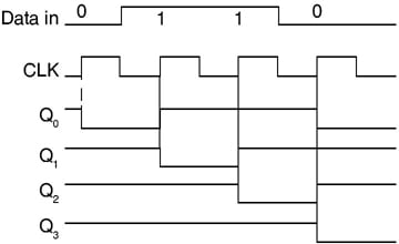
The circuit of a serial-in/parallel-out register using D flip-flop and block symbol of 4-bit SIPO is shown in figure (a) and (b) respectively. It is similar to a serial in serial out (SISO) register the only difference being the manner by which the output is taken out of the register. The data is entered serially one bit/pulse and all the 4-bit data is loaded into the register. Now the output can be read simultaneously through AND gate that helps in storing the data to be taken out of the register.

The waveform of the serial in parallel out 4-bit register is shown in figure below. The serial in parallel out register also requires 4 pulses to load the input data, i.e., one pulse for each bit.
Parallel In/Serial Out (PISO) Shift Register:
A parallel in/parallel-out register has parallel data inputs. The bits are entered simultaneously into their particular stages through parallel lines instead of a bit-by-bit entry as in the case with serial data inputs. The serial output is taken out in the same way as described before. This register can be constructed either using DFF or SR flip-flop. A 2-bit (PISO) register using D flip-flop is shown in the figure below.

Parallel In/Parallel Out Shift Register (PIPO):
The parallel in/serial-out shift register can also be used as PIPO by taking the output, while the parallel output enables line is HIGH. The data can enter and leave the register at the same time.

Bidirectional Shift Registers
In a bidirectional shift register, the stored data can be shifted either from left to right or right to left. Two separate input terminals are present which are used for serial input to be shifted to the right to left and one for data to be shifted left to right by changing the shift. Inputs between logic levels the direction in which the data is shifted can be determined.
The logic level for the data to be shifted to the right and data to be shifted left are complementary to each other. When shift right is at logic 1 the top most AND gates are enabled. This is given to the first flip-flop A, the output of flip-flop A is connected to AND gates. Its output is connected to the D terminal of flip-flop B and so on. This will shift the serial input data to the right as shown in the figure below.
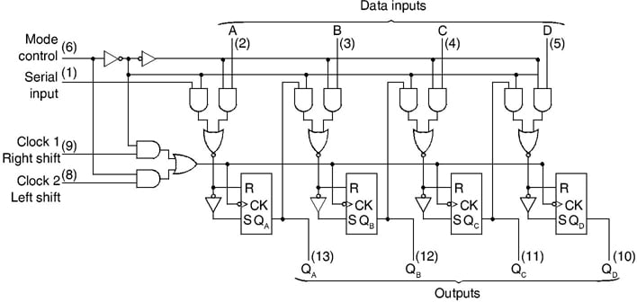
Universal Shift Register
A register in which entering and removing data by all four methods (SISO, SIPO, PIPO, PISO) besides shifting the data from left to right or right to left is called a universal shift register. IC 7495 is a 4-bit universal shift register. The logic symbol is shown in the figure below.

It has 4 input and the corresponding outputs QA, QB, QC, and QD are taken to be low when rest is 0 irrespective of the other inputs. When clock = 0, the outputs are in the previous state S1 and S0 however determine the output. S0 = S1 = 1, the register works in PIPO mode. The data at the serial input is avoided and only the data at parallel input will be considered. This data will appear at the corresponding parallel outputs for positive edge trailing of the clock pulse. S0 = 1, S1 = 0, the shift serial right input is activated for every leading clock pulse the existing data is shifted to the successive stage at the right and the data at QD will be lost.
This mode has no effect on the parallel input data. S0 = 0, S1 = 1 the shift serial left input is activated; the existing data shifts one stage to the left. The data at the output QA of the flip-flop moves out of the register. Parallel inputs have no effect. S0 = S1 = 0 when both are low then the outputs remain in their existing states and have no change. This is similar to the hold state.
Applications of shift register
Time Delay
The SISO shift register is used to provide a time delay from input to the output. If N is the number of flip-flop and fC is the clock frequency, then time delay is given by
This delay depends on the number of flip-flops used by the register and the time period of the clock pulse.
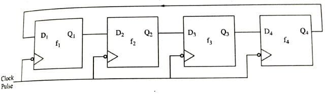
Ring Counter
The basic principle of using shift registers as counters is its use as a feedback loop. The normal output from the previous register is fed to the input of the successive register. Hence it works as SISO register.
It is a shift register in which output of last stage is feedback to input of first stage. This arrangement using D flip-flop is shown in figure below.
Johnson Counter
The Johnson ring counter is similar to the ring counter and is also known as the “Twisted Ring Counters” or “Switch Tail Ring Counters”. The complementary output of the last stage is connected to the J input of the first stage or flip-flop and the output Q is connected to the K input of the first JK flip-flop. A Johnson counter can also be constructed using a D flip-flop. The complemented output of the last stage is connected to the D input of the first JK flip-flop. Since the connections are done from the complementary terminals to the inputs and also the output is measured in the last or tail stage, it is called switch tail ring counters. In some cases, the outputs can be measured from intermediate stages.