Table of Contents
Gate Turn Off (G.T.O.) Thyristor
Gate Turn Off (G.T.O.) Thyristor: A gate turn-off thyristor, a pnpn device, can be turned on like an ordinary thyristor by a pulse of positive gate current. In inverter and chopper circuits, a thyristor can be turned off by forced commutation. For such applications, a GTO is, however, a more versatile device; it can be easily turned off by a negative gate pulse of appropriate amplitude. GTOs were developed sometimes in. the late 1960s but these could not find commercial use because of certain performance problems. Only recently, modem technology has helped in the improved performance of GTOs and these are now being used in several commercial inverters.
As no forced commutation circuitry is required for GTOs, inverters using these devices are compact and cost less. The negative gate current required to turn off a GTO is quite a large percentage (20 to 30%) of anode current prior to commutation. For example, an 800 A GTO will require a negative current pulse of 200 A peak for turning it off. Three circuit symbols of a GTO are shown below. The first & second symbols are self-explanatory, gate current can go in for turning on and out for turning off. But the third symbol looks easy when circuit configurations using GTOs are to be drawn.

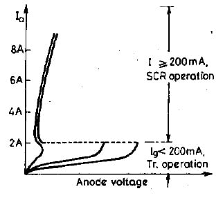
Static V-I Characteristics of GTOs
Typical static V – I characteristics for a GTO thyristor are shown in figure below. It is seen from these characteristics that latching current for large power GTOs is several amperes (here 2A) as compared to 100-500 mA for conventional thyristors of the same rating. If gate current is not able to turn on the GTO, it behaves like a high voltage, low gain transistor with considerable anode current. This leads to a noticeable power loss under such conditions.
Switching Performance of Gate Turn Off Thyristor
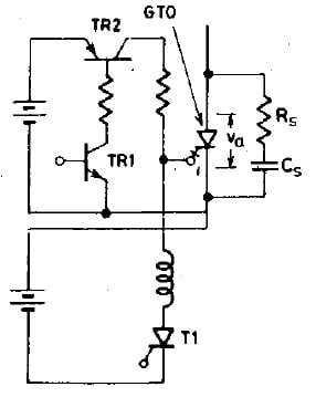
A basic gate drive circuit for a GTO is shown in the figure below. For turning-on a GTO, first transistor TR1 is turned on, this in turn switches on TR2 to apply a positive gate-current pulse to turn on GTO. For turning off the GTO, the turn-off circuit should be oapable of outputting a high peak current. Usually, a thyristor is used for this purpose. The turn-off process is initiated by gating thyristor T1. When T1 is turned on, a large negative gate current pulse turns off the GTO.
Gate turn-on
The turn-on process for a GTO is similar to that of a conventional thyristor. Gate turn-on time for GTO is made up of delay time, rise time, and spread time like a thyristor. Further, turn-on time in a GTO can be decreased by increasing its forward gate current as in a thyristor.
Gate turn-off
The turn-off characteristics of a GTO are different from those of an SCR. Before the initiation of the turn-off process, a GTO carries a steady current Ia, as shown in below. This figure shows a typical turn-off dynamic characteristic for a GTO. The total turn-off time tq is subdivided into three different periods; namely the storage period (ts), the fall period (tf), and the tail period (tt). In other words,
tq = ts + tf + tt
Initiation of turn-off process starts as soon as negative gate current begins to flow after t =0. The rate of rising of this gate current depends upon the gate circuit inductance and the gate voltage applied. During the storage period, anode current Ia, and anode voltage (equal to on-state voltage drop) remain constant. Termination of the storage period is indicated by a fall in Ia , and a rise in Va. During ts, excess charges, i.e. holes, in p-base are removed by negative gate current and the center junction comes out of saturation. In other words, during storage time ts, the negative gate current rises to a particular value and prepares the GTO for turning-off (or commutation) by flushing out the stored carriers. After ts anode current begins to fall rapidly and anode voltage starts rising. As shown in the figure below, the anode current falls to a certain value and then abruptly changes its rate of fall. This interval during which anode current falls rapidly is the fall time tf, and is of the order of 1 µsec. The fall period fall time tf is measured from the instant gate current is maximum negative to the instant anode current fells to its tail current.
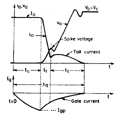
At the time t = ts+ tf, there is a spike in voltage due to abrupt current change. After tf anode current ia and anode voltage Va, keep moving towards their turn-off values for a time tt called tail time. After tt, anode current reaches zero value and Va undergoes a transient overshoot due to the presence of Rc, Cs, and then stabilizes to its off-state value equal to the source voltage applied to the anode circuit. Here Rs and Cs are the snubber circuit parameters. The turn-off process is complete when tail current reaches zero. The over shoot voltage and tail current can be decreased by increasing the size of Cs, but a compromise with snubber loss must be made. The duration of tt depends upon the device characteristics.
Disadvantages
GTO has the following disadvantages as compared to a conventional thyristor :
- Magnitude of latching and holding currents is more in a GTO.
- On state voltage drop and the associated loss is more in a GTO.
- Due to the multicathode structure of GTO, triggering gate current is higher than that required for a conventional SCR.
- Gate drive circuit losses are more.
- Its reverse-voltage blocking capability is less than its forward-voltage blocking capability. But this is no disadvantage so far as inverter circuits are concerned.
Advantages
In spite of all these demerits, GTO has the following advantages over an SCR :
- GTO has faster switching speed.
- Its surge current capability is comparable with an SCR.
- It has more di/dt rating at turn-on.
- GTO circuit configuration has lower size and weight as compared to SCR circuit unit.
- GTO unit has higher efficiency because an increase in gate drive power loss and on-state lose is more than compensated by the elimination of forced commutation losses.
- GTO unit has reduced acoustical and electromagnetic noise due to elimination of commutation chokes.