Table of Contents
Insulated Gate Bipolar Transistor (IGBT)
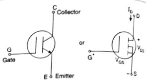
There are numerous types of power semiconductor switches and among these switches, the insulated gate bipolar transistor (1GBT), which combines some of the features of a BJT, a MOSFET, and a thyristor. The figure shown below two different symbols for it. Its terminals are called a gate, collector, and emitter. In another version, they are designated as gate, drain, and source.
The IGBT possesses the following properties:
- It has a high impedance gate as in the case of a MOSFET.
- IGBT possesses low ON-state voltage as in the case of s BJT.
- It can block negative voltages as in the case of a GTO.
In the case of an IGBT, the gate drives are simple and have high switching speed. It has power circuit integration ability and snubberless operation. It is normally useful for AC motor drives, UPS systems, switched mode power supplies (SMPS), A 600 V, 50 A device has an on state voltage drop of 3.2 volts only.
Basic Structure of Insulated Gate Bipolar Transistor (IGBT)
The basic structure of IGBT is shown in figure (a) as shown below. Its structure is similar to that of the vertical DMOS structure of MOSFET but the only difference is the substrate used in IGBT is p-n, whereas, in MOSFET, it is n-n (From the vertical cross-section view it is clear that the collector C is also called drain of IGBT).
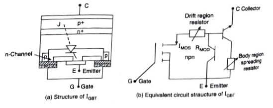
The equivalent circuit for IGBT is shown in above figure (b). The collector terminal is also called a drain. The figure (b) shows the undesirable and unavoidable structure operation during the conditions when the gate does not have control of collector current, the latch up condition will be formed by parasitic thyristor, only forced commutation technique is used to make IGBT turn off under above conditions. There are more changes resulting from destroying of IGBT by the excessive power dissipation in case latch-up condition is not ended with short period of time. In order to reduce latch up, the loop gain αpnp + αnpn, should be made less than one. This condition can achieved by making n buffer and a lifetime control is exercised to reduce αpnp gain and αnpn gain by making appropriate relative doping levels and also emitter shorting (RDS).
IGBT Characteristics (Static V-I Characteristics)
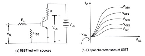
The static V-I characteristics of IGBT are shown in figure (b) below when it is fed with sources as shown in figure (a) below, which are similar to that of a power MOSFET. Expect for p+ substrate, the silicon cross-section of an IGBT is almost identical to that of a power MOSFET.
The behavior of IGBT is closer to a BJT than to that of a power MOST FT because, in the forward direction, its characteristics resemble bipolar junction transistor and moreover due to the presence of a p+ substrate, which forms a PN-junction (p+ substrate and n- drift). Hence, this is a voltage-controlled device that is controlled by input voltage VGE but not by gate current (IG). From figure (b), it can be observed that the relation between IC and VGE is linear, i.e., a straight line but lowest value range of VGE and IC, it is not linear.
Safe Operation Area (SOA) of IGBT
IGBT is safely operated during switching periods. There are two safe operation areas for IGBT. These are FBSOA (forward bias safe operation area) and RBSOA (reverse-bias safe operation area). But these RBSOA is not used in IGBT because reverse bias is not done in IGBT.
The safe operating area (SOA) of an IGBT describes its capability to withstand high levels of voltage and current out the same time. Like other minority carrier devices, uneven current distribution may take place within the die beyond the safe limit. It may cause device failure. A safe operating area (SOA) of an IGBT is similar to a power MOSFET. According to the positive and negative rate of change of current (di/dt), forward-biased SOA (FBSOA) and reverse-biased SOA (RBSOA) are defined respectfully.
Thus FBSOA related to the turn-on transient of the inductive load switching and RBSOA is related to turn-off transient. It is to be noted that the square-SOA or snubberless switching SOA (SSSOA) only gives the absolute maximum current and voltage rating of the device as shown in figure (a) below. However during turn-off. VCE exceeds the dc-supply voltage (VDC), because of the dc-loop inductance ( VL=Ldi/dt). Similarly, during turn-on, the collector current exceeds the output current (I0), because of the reverse recovery current of the diode.

However, in the case of switching an IGBT with a snubber circuit, the voltage and current stresses are greatly reduced as shown in figure (b) above. Similarly, in the case of zero-voltage switching (ZVS)/zero current switchings (ZCS) of the device, these stresses are further reduced. Therefore, a designer should know the worst-case dynamic switching load-lines without a snubber circuit and with a snubber circuit. The dynamic switching load line should fit within the SOA. Moreover, the effective SOA or RBSOA becomes wide for higher frequency as shown in figure (c) above, and the edge is a conditionally defined i.e., frequency-dependent switching SOA.
Applications of Insulated Gate Bipolar Transistor (IGBT)
IGBTs are widely used in medium power applications such as dc and ac motor drives, UPS systems, power supplies, and drives for solenoids, relays, and contractors. Though IGBTs are somewhat more expensive than BJTs, yet they are becoming popular because of lower gate-drive requirements, lower switching losses, and smaller snubber circuit requirements. IGBT converters are more efficient with less size as well as cost, as compared to converters based on BJTs. Recently, IGBT inverter induction-motor drives using 15-20 kHz switching frequency are finding favor where audio-noise is objectionable. In most applications, IGBTs will eventually push out BJTs. At present, the state of the art IGBTs is available up to 1200 V, 500 A.
