Table of Contents
Transistor-Transistor Logic (TTL)
TTL as outlined above stands for Transistor-Transistor Logic. It is a logic family implemented with bipolar process technology that combines or integrates NPN transistors, PN junction diodes, and diffused resistors in a single monolithic structure to get the desired logic function. The NAND gate is the basic building block of this logic family.
Transistor-Transistor Logic is the most popular and widely used IC logic family. It is also known as T2L family and was introduced by Texas Instruments in 1964.
Working of Transistor-Transistor Logic (TTL)
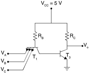
The circuit of the basic Transistor-Transistor Logic (TTL) gate is shown in the figure below. Let us first consider the working of the basic TTL gate. When the input voltage is high, then transistor T1 will be in the reverse active region. The base-emitter voltage is less and the base-collector voltage, VBE, will be more than zero. The current from VCC will flow across the base resistor RB. It later passes through the collector-base junction of T1 and into the base of transistor T3. Transistor T3 is saturated and the output of the gate is 0.2 V.

When the input voltage is low, then the base-emitter voltage VBE is more than zero thereby making the current flow through the base resistor to the emitter-base junction of T1 and then to the ground. The charge stored at the base of the transistor T3 does not leak through the resistor instead flows across the forward-biased collector-base junction of transistor T1. This drives the transistor T1 to cut-off. Now the output voltage is high approximately +5 V.
The main difference between the DTL and TTL logic families lies in the operational speed. The transition speed from logic high to low depends on the speed at which the charge is dissipated. The charge stored in the base has a higher discharging current compared to the DTL gate. Thus, the TTL is much faster than DTL.
Multi-Emitter TTL Gate:
Consider a 3-input TTL NAND gate with a simple output stage. The inputs are applied across emitters of a multiple-emitter transistor. The circuit is shown in the figure below. When all the inputs are held at high it causes the base-emitter junctions of the multiple-emitter transistor to be reverse-biased. A small collector current due to the reverse biasing of the transistor is available at the inputs. The positive voltage from VCC flows through the base resistor RB into the base of the transistor T1. This current passes through the base-emitter junction of the output transistor. Thus, the output transistor conducts and the output voltage low or logic 0.
When one of the inputs to the multi-emitter transistor T1 is at logic 0, then no current flows through the base of the output transistor and the output voltage is high. This is because the base-collector junction of transistor T1 and the base-emitter junction of the output transistor is connected in parallel across the resistors and ground. When two such stable voltage components having different threshold voltages are connected in parallel, then the current flows across the path with less threshold voltage. This is known as current steering. The same phenomenon occurs when one of the inputs is given logic 0. No current flow is observed at the base of transistor T3 thereby making the transistor reach the cut-off state. The output voltage is high, i.e., logic 1.
Disadvantage of Single Output Stage TTL:
The output resistance is extremely high when the output is logic 1. Also this is completely determined by the output collector resistor. The high output resistance restricts the number of inputs that can be connected.
Totem Pole Transistor-Transistor Logic (TTL):
The main disadvantage of TTL is the high output resistance of the single output stage. This is overcome using the “totem-pole” TTL gate as shown in the figure below. It consists of the two NPN transistors T3 and T4, the diode D1, and the current-limiting resistor R3. The gate is driven by applying the same current steering idea as above.
When the transistor T2 is off then this makes transistor T4 also to be in the off state. Transistor T3 operates in active region and produces high output voltage. When the transistor T2 is on then this makes transistor T4 also to be in on state. This causes a low voltage at the output. It is evident from the circuit that the base-emitter of T3 and diode are connected in series. To this series connection, the collector-emitter junction of transistors T2 and T4 are connected. When the base current of transistor T3 is low it drives the transistor to a cut-off state.
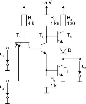
The resistor R3 controls the flow of current through the transistor T3, diode D1 and transistor T4 that are connected in series when all are in the conducting state. The output current is also controlled. The resistor R3 decreases the output resistance as it is connected to the collector of transistor T3. Thus, these resistors also known as pull-up and pull-down resistors can be removed from the output stage to increase the strength of the gate without affecting the power consumption. The main advantage of TTL with a “TOTEM-pole” output stage is the low output resistance at output logical “1”.
The TTL has many subfamilies having standardized labeling system starting with 54 or 74. Some of the subfamilies of TTL are shown in the Table below.