Table of Contents
Schottky Barrier Diode
Schottky Barrier Diode is a simple metal-semiconductor interface exhibiting anon-linear impedance and is basically an extension of the point-contact diode. When the diodes are forward biases current flows because of majority carriers from semiconductor into the metal. Minority carriers are virtually absent compared with p-n junction diodes. These diodes have very less reverse recovery times and almost nil storage capacitance.
Silicon is most commonly used although GaAs find use at higher frequencies. Schottky Barrier Diode has its main applications in microwave detection and mixing. Available SBD’s have a frequency range up to 100 GHz and noise figures of 4 dB at 2 GHz and 15 dB at 100 GHz. At still higher frequencies (1000 GHz to 2000 GHz), point contact diodes have an edge over SBD’s because of their lower shunt capacitance. They can be used as both varactors over a wide frequency range.
This diode is formed by the junction of a semiconductor and a metal. This junction has unipolar properties. Aluminum is generally used.
Construction
A Schottky Barrier Diode consists of a metal base on which a silicon pellet is mounted. A spring-loaded wire with a sharp point makes contact with the polished surface of the semiconductor pellet. The other connections are made as shown below. Such construction can be easily mounted into co-axial or waveguide lines. They are noisier above 10 GHz.

There I-V and C-V characteristics are similar to those of p-n junctions, but have steeper I-V slope, lower series resistance R, lower breakdown voltage, and smaller forward turn-on voltage.
Working of Schottky Barrier Diode
The Schottky diode is as shown in the figure below. It contains a junction between an n-type semiconductor and a metal. Initially, when no bias is applied, electrons from the conduction band of the N-type semiconductor reach the metal, leaving a region known as the depletion layer that has no free electrons. This results in the buildup of a positive space charge region in the semiconductor, because each donor atom loses an electron and, hence, becomes positive. This results in the buildup of an electric field that opposes the further flow of electrons to the metal. Since the metal contains a greater number of free electrons, the depletion width inside it is small.
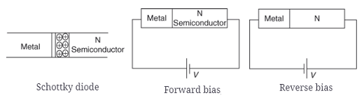
In the forward-biased condition, the metal is biased positively with regard to the semiconductor. Then, a few electrons from the N-type semiconductor whose thermal energy happens to be many times the average thermal energy will fall down from the potential barrier and move into the metal. Therefore, these electrons are known as hot electrons. Merely those electrons are considered for the forward currents from the semiconductor into the metal. These will have higher energy and velocity till they come into equilibrium with the free electrons of the metal. This raises the temperature of the diode and is, therefore, called a hot carrier diode.
An important feature of this diode is that there is no flow of holes from the metal into the semiconductor. Therefore, there is no hole-electron recombination (that takes place in a conventional PN diode). Therefore, if the forward voltage is removed, the time taken by the current to stop is in the order of a few picoseconds, and reverse voltage can be established at this time. As in junction diodes, there is no delay effect due to charge storage.
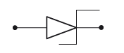
Equivalent circuits
The equivalent circuit and electronic symbol of a Schottky diode are as shown in the figure below.
These parameters are as follows:
- The series inductance, Ls, is the inductance of the bonding wires. It has typical values of 0.4 to 0.9 nH.
- The series resistance in the Schottky diode is the total resistance in the diode, including that of the semiconductor and the substrate on which the diode is mounted. This value is particularly important when we are choosing a diode for a detector or a mixer application. Its value ranges from 4 to 6 ohm.
- The junction capacitance is the capacitance that is present across the actual junction between the semiconductor and the metal. It ranges from 0.3 to 0.5 pF.
- Rj is the junction resistance, that is, the resistance of the area where the semiconductor and the metal come together.
- The overlay capacitance, Co, is the value of capacitance produced from the Schottky junction to the metal contact of the opposite lead of the diode.

Applications
- They are used in fast-switching applications such as in microwave mixers, where the diode should switch conductance states at the rate of the frequency of a microwave local oscillator.
- A Schottky diode is used as a square-law detector when bias is zero, whose power output is proportional power to input.
- They are used in detectors.

