Table of Contents
Demultiplexer
Definition: A Demultiplexer Commonly termed as DEMUX does the opposite of MUX, i.e., it receives information on a single line and transmits this information on one of the 2n possibles output lines.
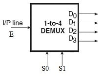
Demultiplexers are those that perform the inverse of the multiplexing operation on a given function. They are abbreviated as DEMUX. It has one input line (E) and transmits it to one of 2n possible output lines (D0, D1, D2 …, D2n – 1). The specific output is selected based on the bit combination of n select inputs. The basic diagram of a DEMUX is shown in the figure below.

A decoder is a special case of a demultiplexer without the input line.
The basic design of demultiplexer
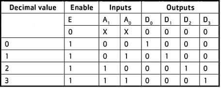
The basic design and working of a DEMUX can be understood from the following example. Consider a 1-to-4 line demultiplexer. The circuit representation and truth table of a 1-to-4 line demultiplexer when the input line is held HIGH is shown below.

It has two select lines, S1 and S0. The input E is applied to one of the outputs and is specified by the two select lines, S1 and S0. When the select lines are given the values as shown then the output is given according to the Table shown below.

2-to-4 decoder
A demultiplexer is identical to a 2-to-4 decoder with enable input figure below.
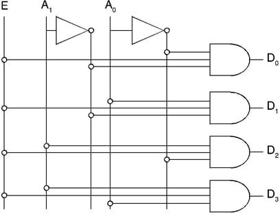
In the case of a decoder, the inputs are A1 and A0, and the enable is input E. But in demultiplexer, the input E provides the data, while other inputs accept the selected variables. Both the circuits have different applications yet their logic diagrams are exactly the same.
Consider the 74LS or 74HC139 which are examples of 1-to-4 line demultiplexers/decoders. Both the ICs have single enable and two input select pins. There are 4-output pins. When logic HIGH is applied to the enabling, then all the four outputs are high regardless of the state of the select pins. When a logic LOW is applied to the enabling then the outputs chosen by the address pins A and B will be LOW and other outputs will be HIGH. Consider the truth table of a 1-to-4 line DEMUX as in the table below.
Thus, the enable pin defines whether the circuit functions as a demultiplexer or decoder. When the enable pin functions as a data input pin then it is a demultiplexer. When the enable pin is LOW it acts as a decoder.
IC 74LS138 pinout (Demultiplexer IC)
the IC 74LS138/74HC138 has 3-enable inputs out of which one pin acts as data input when the chip functions as a demultiplexer as shown in Figure below.

Cascading Decoder Circuits
There can possibly be a situation where the desired number of input and output lines is not available in IC decoders. More than one of these devices of a given size may be used to construct a decoder that can handle a larger number of input and output lines. For instance, 3-to-8 line decoders can be used to construct 4-to-16 or 5-to-32 or even larger decoder circuits. The basic steps to be followed to carry out the design are as follows:
- If n is the number of input lines in the available decoder and N is the number of input lines in the desired decoder, then the number of individual decoders required to construct the desired decoder circuit would be 2N−n.
- Connect the less significant bits of the input lines of the desired decoder to the input lines of the available decoder.
- The left-over bits of the input lines of the desired decoder circuit are used to enable or disable the individual decoders.
- The output lines of the individual decoders together constitute the output lines, with the outputs of the less significant decoder constituting the less significant output lines and those of the higher-order decoders constituting the more significant output lines. The concept is further illustrated in solved example 8.8, which gives the design of a 4-to-16 decoder using 3-to-8 decoders.
Example
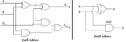
Implement a full adder circuit using a 3-to-8 line decoder.
Solution
A decoder with an OR gate at the output can be used to implement the given Boolean function. The decoder should at least have as many input lines as the number of variables in the Boolean function to be implemented. The truth table of the full adder is given in the table and the hardware implementation is shown below.
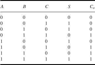

From the truth table, Boolean functions for SUM and CARRY outputs are given by the following equations:
Sum output S = Σ 1, 2, 4, 7
Carry output C0 = Σ 3, 5, 6, 7
Related Post:
Multiplexer and implementation