
Table of Contents
Vidicon camera tube
The Vidicon camera tube is based on the photoconductive properties of semiconductors. When light falls on it, the number of free electrons created at any point is directly proportional to the intensity of light falling on that point. A photo-conductive property of semiconductors means a decrease in resistance with the amount of incident light. Brighter the light, greater is the number of free electrons. These electrons are removed from the material by using a positive voltage and hence that becomes positively charged. The value of charge on the target at any point is proportional to the intensity of light at the corresponding point in the original scene. So, the charge image of the picture is formed on the surface of the target.
The Vidicon camera tube was the first camera tube based on the photoconductive principle and is developed by Radio Corporation of America (RAC) in the early 1950s and gained immediate popularity because of its small size and ease of operation.
Construction of Vidicon Camera Tube
The Camera Tube structure is illustrated is shown in the figure below. It consists of :
(i) Target Plate or Signal Plate
(ii) Scanning System

(i) Target Plate or Signal Plate
The target consists of a thin conducting metallic film of the photoconductive layer, so as to be transparent. The side of these films facing cathode is coated with a very thin layer of photo-conductive material i.e. either selenium or antimony compounds. This is deposited on a transparent conducting film, coated on the inner surface of the faceplate. This conductive coating is known as a signal electrode or plate. This side is scanned by the electron beam. The optical image is focused on the other side of this film.
The photoconductive target material is an intrinsic semi-conductor that has a very high resistivity in darkness and is decreasing it with an increase in illumination. The photo layer has a thickness of about 0.0001 cm and behaves like an insulator with a resistance of approximately 20 MΩ when in dark. When bright light falls on any area of the photoconductive coating, resistance gets reduces to about 2 MΩ. Very few charge leaks between the successive frames and this change are stored by the beam and the resulting current to the electrode is called dark current.
(ii) Scanning System
The electron beam for scanning is formed by the combination of the cathode, control grid (Grid no. 1), accelerator (Grid-2) and anode (Grid-3). The focusing coil produces an axial field which focuses the beam on the film. Vertical and horizontal deflection of the beam, so as to scan the whole film, is accomplished by passing sawtooth current waves through deflecting coils which thus the produce transverse horizontal and vertical magnetic field respectively the alignment coil are for initial adjustment of the direction of the electron beam.
Working of Vidicon camera tube
When the scanning beam passes over the photo-conductive material of the signal plate, it deposits electrons so that the potentials of this side of the plate are reduced to that of the cathode. But the other side of the film (plate) is still at its original potential consequently a potential difference across a given point on the photo-conductive material is created. It is approximately 40 V. Before the next scanning (which may be done after an interval of 1/50 or 1/25 sec.), the charge leaks through photoconductive material at a rate determined by the conductivity of the material which in turn, depends upon the amount of incident light. White portions of the object will, in turn, depends upon the film and make it more conductive.

This change leaked to the photoconductive side of the film will vary according to the illumination of the object. As a result potential at every point on the photoconductive side of the film but this time the charge deposited by the beam in order to reduce its potential towards zero (cathode potential) will vary with time. Therefore current through load resistance (RL) will follow the changes in the potential difference between two surfaces of the film and hence follow the variation of light intensity of successive points in the optical image.
Storage Action
Since the light from the picture is continuously falling on the target, each element of the photo coating is scanned at an interval equal to the frame time i.e. 1/50 sec. This results in storage action and the net change in resistance, at any point or element on the photoconductive layer. It depends on the time and the light information at each element or pixel is thus integrated over the time elapsed between the samples, Then it is stored in the form of light-dependent positive charge image pattern on the cathode side of the plate. The storage time is the same for all points on the target plate. The net change in resistance of all elementary areas is proportional to light intensity variations in the scene being televised.
Leaky Capacitor Concept
There is another way of explaining the development of ‘charge image’ on the photo layer is to consider that it is an array of individual target elements. Each element consists of a capacitor parallel with a light-dependent resistor. As seen there, one end of these target elements is connected to the signal electrode and the other end is unterminated facing the beam. In the absence of any light image, the capacitors attain a charge almost equal to the + 40 V, in the absence of any light image. However, when an image is focused on the target, the resistors in parallel with the capacitors change in value depending on the intensity of light on each unit element. For a high light element, the resistance across the capacitor drops to a fairly low value, and this permits a lot of charge from the capacitor to leak away.

At the time of scanning, more electrons are deposited, on the unterminated end of this capacitor to recharge it to the full supply voltage of + 40 V. The flow of current that completes its path through RL develops a signal voltage across it. Similarly, for black areas of the picture, the resistance across the capacitors remains high, and not much charge is allowed to leak from the corresponding capacitors. This, in turn, needs a fewer number of electrons from the beam to recharge the capacitors. The resultant small current that flows, develops a lower voltage across the load resistance.
The electron beam thus ‘sees’ the charge on each capacitor, while scanning the target, and delivers more or less number of electrons to recharge them to the supply voltage. This process is repeated every 40 ms to provide the necessary video signal corresponding to the picture details at the upper end of the load resistor. The video signal is fed through a blocking capacitor to an amplifier for necessary amplification.
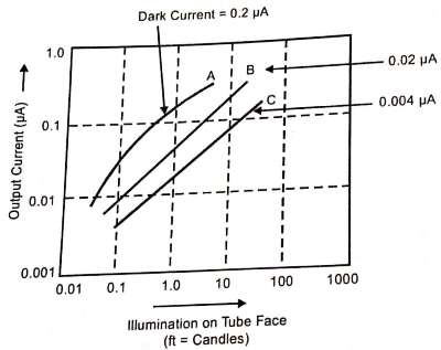
Light Transfer Characteristics
In the absence of illumination on the faceplate, there is some discharge of the pixels capacitors having some finite value of the resistance of the photoconductive layer. It produces some recharging signal current in the dark condition also, known as dark current. The vidicon output characteristics curve is shown below figure. Each curve is for a specific value of ‘dark’ current, which is the output with no light. The ‘dark’ current is set by adjusting the target voltage. Sensitivity and dark current both increase as the target voltage is increased. The typical output for the vidicon is 0.4 µA for bright light with a dark current of 0.02 µA.
High Image Lag
This camera tube suffers from image lag. The photoconductive layer has a finite time lag, which can cause shear with a trail following fast-moving objects. The photoconductive lag increases high target voltage, where the vidicon has its highest sensitivity.
Applications of Vidicon camera tube
This tube is quite popular for CCTV (Closed Circuit Television) applications because of low cost, small size, simplicity and ease of operations. Some more applications of the vidicon camera tube are as follows:
- Widely used for outdoor recording, domestic and industrial recording.
- Aerospace and oceanography.
- It is also used in slides, pictures, medicine, education, etc.
- It is the most popular tube in the television industry.
Advantages
- No ghost image.
- There is no halo effect.
- It is low cost and simple.
- No gamma corrections needed.
- Signal response is close to the human eyes.
- It has a long life of about 5000 to 20,000 hours.
- It is compact, having a length of 12-20 cms and a diameter of 1.5-4 cm.
- By varying the target voltage as per the illumination of the scene, sensitivity can be adjusted.
- Resolution is better than ortiocon. Resolution in order of 350 lines can be achieved under practical conditions.
Disadvantages
- Image lag is severe.
- Dark Current is high approximately 20 µA.
- Sensitivity is less than image orthicon.
- The response characteristics are non-linear.

