Table of Contents
Tunnel Diode
Tunnel diode is a specially made p-n junction device which exhibits negative resistance over part of the forward bias characteristics. It has extremely heavy doping on both sides of the junction and an abrupt transition from the p-side to the n-side. The tunneling effect is a majority carrier effect and is consequently very fast. The tunnel diode is useful for the oscillation of amplification purposes. Because of the thin junction and short transit time, it is also useful for microwave applications in fast switching circuits.
In 1958, Leo Esaki, a Japanese scientist, discovered that if a semiconductor junction diode is heavily doped with impurities, it will have a region of negative resistance. The normal junction diode uses semiconductor materials that are lightly doped with one impurity atom for ten-million semiconductor atoms. This low doping level results in a wide depletion region.
Working Principle of Tunnel Diode
“Fermi level is defined as the energy state with a 50% probability of being filled if no forbidden band exists.” The Fermi level for an intrinsic semiconductor would be almost midway between the valence and conduction bands for an intrinsic semiconductor. When the impurities are added to the semiconductor to convert to the extrinsic type, this Fermi level shifts up or down. If the acceptor atoms are added to make the semiconductor p-type, the Fermi level is shifted towards the valence band and is just above the valence band. For an n-type semiconductor, this Fermi level will shift up towards the conduction band. The complete energy-band diagram, including the Fermi level for an ordinary diode, is shown in the figure below The Fermi level on both sides of the diode is seen to be at the same level and lies in the forbidden gap on both sides of the junction.
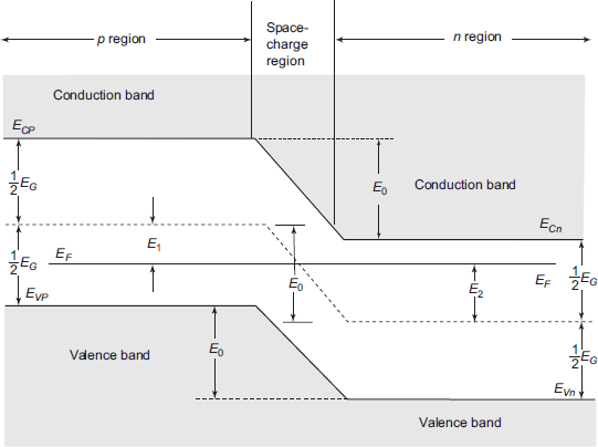
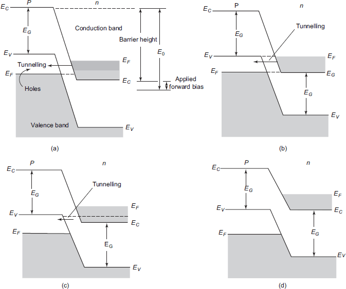
Energy diagram of Tunnel Diode for open circuit
As seen in the figure below, the Fermi level is no more in the forbidden gap of the energy band for a highly doped tunnel diode. The Fermi level is pushed to the valence band in the p region and is in the conduction band of the n region. The Fermi level is at the same energy level on both sides of the diode when the diode is open-circuited. In the p region of a tunnel diode, there is an empty space above the Fermi level in the valence band where electrons can exist.

But, in the n region of the diode, the valence band is totally full and electrons available up to the Fermi level in the conduction band as shown in the figure. There are electrons in the conduction band of n region and also electrons in the valence band of the p region of the same energy levels in this diode. Since the depletion layer is extremely thin, those electrons above the conduction band in the n region penetrate through the depletion layer to reach the p region.
The electrons in the valence band of the p region, which are having energies above the conduction band of n region cross the junction to reach n region. Thus, the electrons travel in both the directions and at equilibrium, the number of electrons passing from p side to n side would be the same as those from the opposite direction. Thus, the effective current in the device is zero.
Energy diagram of Tunnel Diode for reverse bias
When the diode is reverse biased, the contact potential is raised by the amount of the applied reverse voltage. This corresponds to a raise in the difference of energy levels between the p side and n side of the diode as shown in figure (b). The energy difference will be more than EG. Assuming the levels in the p region to be intact (at a potential zero), the energy level in the n region comes down.
It is now observed that there are some energy states in the valence band of the p side which lie at the same level as allowed empty states in the conduction band of the n side. That is, there are electrons in the p side with energies higher than the filled energy states in the conduction band of n side. Thus, the electrons on the p side can tunnel through the depletion layer to reach and occupy the unfilled energy states of the conduction band of n side.
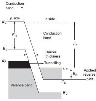
Thus, the number of electrons moving from p to n side is more compared to the electrons moving in the opposite direction. This leads to a flow of conventional current from n side to p side of the diode. As the applied reverse potential increases, the difference of energy levels on the p and n sides increases and more and more electrons tunnel from n to p side, thus increasing the current in the diode. This leads to a linear relationship between the current and applied potential in the reverse direction in contrast to the constant current, as observed in an ordinary p-n junction diode. The characteristic of this behavior is depicted in the plot of the V-I characteristic of the tunnel diode.
Energy-band diagram (EBD) of tunnel diode
Consider that the diode is in forward bias now and the change in the energy-band structure of the tunnel diode is as depicted in the figure below (figure a, b, c & d). When a small voltage is applied to the diode to forward bias, the energy state difference between the p and n sides decreases correspondingly as shown in figure (a).
Now, the energy state difference between the p and n sides of the diode would be less than EG. Thus, there are electrons in the conduction band of n region, which are at a higher potential than the maximum filled energy levels in the valence band of p region. These electrons can now tunnel through to reach the p region and thus there is an effective electron current flowing from n to p side of the diode. Thus, conventionally, the current flows from p to n side of the diode. As the forward voltage to the diode is increased, a number of electrons can tunnel through the depletion layer and the current increases linearly until a point is reached as shown in figure (b), where maximum current flows in the diode. So, the current increases almost linearly with voltage until this point.
When the voltage is increased beyond this point, as depicted in figure (c), all the electrons available in the conduction band of n side will not be able to tunnel towards the p side since there exists a forbidden energy gap corresponding to the energy states higher than the valence energy band of p side. Thus, the electrons in the conduction band of n side with energies higher than the valence energy band of p side cannot tunnel through since there exists a forbidden energy gap corresponding to these electron energy states. Thus, fewer electrons cross the junction and the current decreases. As the voltage is further increased, the electrons crossing the junction decrease further and the current is lowered with voltage. This is as represented in the V-I Charecterics Curve. In this region, as the voltage is increased, the current decreases. This is referred to as negative resistance region.
This decrease in current continues as the voltage is increased until a point is reached where all the electrons in the conduction band of n side are at energy states corresponding to the forbidden gap of the p side. At this juncture, as shown in figure (d), no current flows in the diode. Above this voltage, the band structure of an ordinary p-n junction diode, as shown in the energy-band diagram of a p-n junction diode.
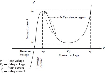
Tunnel Diode Characteristic Curve
Tunnel Diode’s voltage versus current characteristic is shown in the figure below. The electric field at the junction will be very large and the conditions become favorable for electrons on the N-material side for tunneling through the energy barrier and spontaneously appear on the P-material side. Such devices are called tunnel diodes.
As seen from the V–I characteristic of a tunnel diode, the diode conducts as a linear resistor when reverse biased and exhibits negative resistance when forward biased. The voltage at which the maximum current flows before the negative resistance region is known as peak voltage VP and the corresponding current as peak current IP. The voltage at which minimum current flows in the diode, when forward biased, is valley voltage VV and the corresponding current is valley current IV. Thus, between the current limits IV and IPr, the function is triple valued. That is, the same magnitude of the current can be achieved in the diode for three different voltages in the forward-biased region. This makes the diodes most suitable in the pulse and digital circuits.
The device exhibits negative resistance when biased between VP and VV. This has large applications as an amplifier, oscillator and very fast switch in microwave frequencies. Since tunneling takes place at the speed of light, it acts as a very high-speed switch.
Tunnel Diode and Its Equivalent Circuit
The tunnel diode can be represented by the equivalent circuit, where LS corresponds to the lead inductance, RS, the equivalent series resistance Cj is the junction capacitance, R is the slope of the negative resistance region of the tunnel diode. Typical parameters are indicated on the equivalent circuit shown in the figure.

The frequency of operation of a tunnel diode far exceeds the frequency calculated on the basis of depletion region width; the discrepancy can be explained as follows. The electron hitting one edge of the barrier is supposed to emit a photon, which travels at the speed of light and on arriving at the other edge of the barrier emits another electron. Thus, it is as though the photon is the particle that travels the transition region instead of the electron, which is bulkier, compared to the photon.
Applications of Tunnel Diode
- Oscillators for the UHF range of the order of tens of gigahertz.
- For low access time memories.
- The pressure to current transducers.
- As mixers detectors and converters for UHF receivers.
- As a high-speed switch of the order of nanoseconds switching time.
Advantages
- Low noise figure.
- High-frequency response.
- Lower dissipation.
Disadvantages
- Low voltage and current levels of operation of the device.
- Being a two-terminal device, no isolation between input and outputs.