A microprocessor or 8085 microprocessor is a programmable device that accepts binary data from an input device, processes the data according to the instructions stored in the memory, and provides results as output.
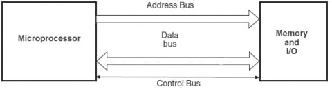
According to other definitions, the microprocessor is a program executing device, which stored the program in memory and provides the result through output and transfer data through I/O ports to the other devices. Any microprocessor-based framework basically includes three sections, to be specific the microprocessor, the memory, and peripheral I/O devices. The microprocessor is the heart of the system or framework as it plays out all the tasks and furthermore controls the rest of the framework. The three sections are interconnected by the data bus, the address bus, and the control bus.

Table of Contents
8085 Pin Diagram | Functional Pin Diagram of 8085 Microprocessor:
Pin Diagram and functional pin diagram of 8085 microprocessor is shown below respectively. The signals of the 8085 Pin Diagram can be classified into seven groups according to their functions.
- Power supply and frequency signals.
- Data bus and address bus
- Control bus
- Interrupt signals
- Serial I/O signals
- DMA signals
- Reset signals
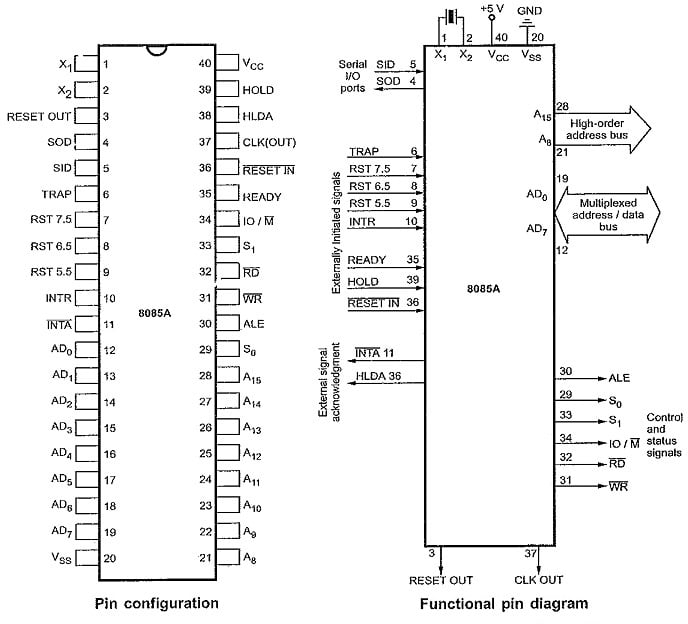
Power Supply and Frequency Signals:
- Vcc : It requires a single +5 V power supply.
- Vss : Ground reference.
- X1 and X2 : A tuned circuit like LC, RC or crystal is connected at these two The internal clock generator divides oscillator frequency by 2, therefore, to operate a system at 3 MHz, the crystal of tuned circuit must have a frequency of 6 MHz.
- CLK OUT: This signal is used as a system clock for other devices. Its frequency is half the oscillator frequency.
2. Data Bus and Address Bus:
A) AD0 to AD7 : The 8-bit data bus (D0 – D7) is multiplexed with the lower half (A0 – A7) of the 16-bit address bus. During the first part of the machine cycle (T1), lower 8 bits of memory address or I/O address appear on the bus. During the remaining part of the machine cycle (T2 and T3) these lines are used as a bi-directional data bus.
B) A8 to A15 : The upper half of the 16-bit address appears on the address lines A8 to A15. These lines are exclusively used for the most significant 8 bits of the 16 bit address lines.
3. Control and Status Signals:
A) ALE (Address Latch Enable) : We, know that AD0 to AD7 lines are multiplexed and the lower half of address (A0 – A7) is available only during T1 of the machine cycle. This lower half of address is also necessary during T2 and T3 of machine cycle to access specific location in memory or I/O port. This means that the lower half of an address must be latched in T1 of the machine cycle, so that it is available throughout the machine cycle. The latching of lower half of an address bus is done by using external latch and ALE signal from 8085 Pin Diagram.
B) RD and WR : These signals are basically used to control the direction of the data flow between processor and memory or I/O device/port. A low on RD indicates that the data must be read from the selected memory location or I/O port via data bus. A low on WR indicates that the data must be written into the selected memory location or I/O port via data bus.
C) IO/M, S0, and S1 : IO/M indicates whether I/O operation or memory operation is being carried out. S1 and S0 indicate the type of machine cycle in progress.
D) READY : It is used by the microprocessor to sense whether a peripheral is ready or not for data transfer. If not, the processor waits. It is thus used to synchronize slower peripherals to the microprocessor.
4. Interrupt Signals:
The 8085 Pin Diagram has five hardware interrupt signals: RST 5.5, RST 6.5, RST 7.5, TRAP, and INTR. The microprocessor recognizes interrupt requests on these lines at the end of the current instruction execution.
The INTA (Interrupt Acknowledge) signal is used to indicate that the processor has acknowledged an INTR interrupt.
5. Serial I/O Signals:
A) SID (Serial I/P Data) : This input signal is used to accept serial data bit by bit from the external device.
B) SOD (Serial O/P Data) : This is an output signal which enables the transmission of serial data bit by bit to the external device.
6. DMA Signal:
A) HOLD : This signal indicates that another master is requesting for the use of address bus, data bus and control bus.
B) HLDA : This active high signal is used to acknowledge HOLD request.
7. Reset Signals:
A) RESET IN : A low on this pin
- Sets the program counter to zero (0000H).
- Resets the interrupt enable and HLDA flip-flops.
- Tri-states the data bus, address bus, and control bus. (Note: Only during RESET is active).
- Affects the contents of the processor’s internal registers randomly.
On reset, the PC sets to 0000H which causes the 8085 Pin Diagram to execute the first instruction from address 0000H. For proper reset operation reset signal must be held low for at least 3 clock cycles. The power-on reset circuit can be used to ensure execution of first instruction from address 0000H.
B) RESET OUT : This active high signal indicates that the processor is being reset. This signal is synchronized to the processor clock and it can be used to reset other devices connected in the system.
8085 Microprocessor Architecture and its Operations:
The 8085 Microprocessor Architecture is shown below. It consists of various functional blocks as listed below :
- Registers
- Arithmetic and Logic Unit
- The instruction decoder and machine cycle encoder
- Address buffer
- Address/Data buffer
- Incrementer/Decrementer Address Latch
- Interrupt control
- Serial I/O control
- Timing and control circuitry
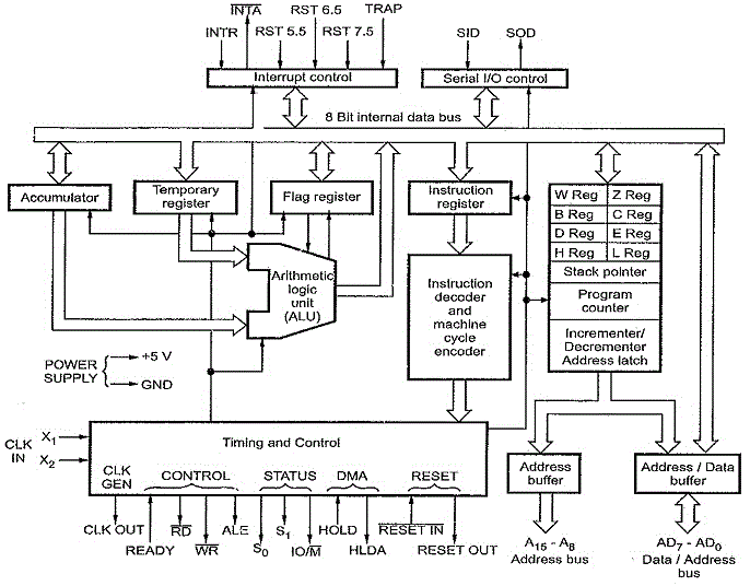
For the detailed discussion of different parts of the architecture of 8085 microprocessor click here.
Features of 8085 microprocessor
The features of 8085 include:
- It is an 8-bit microprocessor i.e. it can accept, process, or provide 8-bit data simultaneously.
- It operates on a single +5 V power supply connected at Vcc; the power supply ground is connected to Vss.
- It operates on a clock cycle with 50% duty cycle.
- It has an on-chip clock generator. This internal clock generator requires a tuned circuit like LC, RC, or crystal. The internal dock generator divides oscillator frequency by 2 and generates a clock signal, which can be used for synchronizing external devices.
- It can operate with a 3 MHz clock frequency. The 8085A-2 version can operate at a maximum frequency of 5 MHz.
- It has 16 address lines, hence it can access (216) 64 Kbytes of memory.
- It provides 8 bit I/O addresses to access (28) 256 I/O ports.
- In 8085, the lower 8-bit address bus (A0 – A7) and data bus (D0, – D7) are multiplexed to reduce the number of external pins. But due to this, external hardware (latch) is required to separate address lines and data lines.
- It supports 74 instructions with the following addressing modes :
- Immediate b) Register c) Direct d) Indirect e) Implied
- The Arithmetic Logic Unit (ALL)) of 8085 performs:
- 8-bit binary addition with or without carry
- 16-bit binary addition.
- 2 digit BCD addition.
- 8-bit binary subtraction with or without borrow
- 8-bit logical AND, OR, EX-OR, complement (NOT), and bit shift operations.
- It has an 8-bit accumulator, flag register, instruction register, six 8-bit general-purpose registers (B, C, D, E, H, and L) and two 16-bit registers (SP and PC). Getting the operand from the general-purpose registers is faster than from memory. Hence skilled programmers always prefer general-purpose registers to store program variables than a memory.
- It provides five hardware interrupts TRAP, RST 7.5, RST 6.5, RST 5.5, and INTR.
- 8085 microprocessor has serial I/O control which allows serial communication.
- It provides control signals to control the bus cycles, and hence the external bus controller is not required.
- It has a mechanism by which it is possible to increase its interrupt handling capacity.
- The 8085 has an ability to share system bus with the Direct Memory Access controller. This feature allows transferring a large amount of data from I/O device to memory or from memory to I/O device with high speeds.
Related Post
RISC and CISC Processors: Architecture and Characteristics
8085 microprocessor architecture
