Table of Contents
8085 Microprocessor Architecture
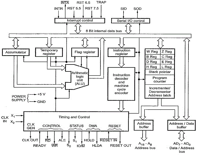
The 8085 Microprocessor Architecture is shown below. It consists of various functional blocks as listed below :
- Registers
- Arithmetic and Logic Unit
- The instruction decoder and machine cycle encoder
- Address buffer
- Address/Data buffer
- Incrementer/Decrementer Address Latch
- Interrupt control
- Serial I/O control
- Timing and control circuitry
8085 Microprocessor Different Parts
Registers:
It has eight addressable 8-bit registers : A, B, C, D, E, H, L, F, and two 16-bit registers PC and SP. These registers can be classified as:
- General Purpose Registers
- Temporary Registers: a) Temporary data register b) W and Z registers
- Special Purpose Registers: a) Accumulator b) Flag registers c) Instruction register
- 16-bit Registers: a) Program Counter (PC) b) Stack Pointer (SP)
General Purpose Registers:
B, C, D, E, H, and L are 8-bit general purpose registers can be used as a separate 8-bit registers or as 16-bit register pairs, BC, DE, and HL. When used in register pair mode, the high order byte resides in the first register (i.e. in B when BC is used as a register pair) and the low order byte in the second (i.e. in C when BC is used as a register pair).
HL pair also functions as a data pointer or memory pointer. These are also called scratchpad registers, users can store data in them. To store and read data from these registers bus access is not required, it is an internal operation. Thus it provides an efficient way to store intermediate results and use them when required. The efficient programmer prefers to use these registers to store intermediate results than the memory locations which require bus access and hence more time to perform the operation.
Temporary Registers:
(a) Temporary Data Register: The ALU has two inputs. One input is supplied by the accumulator and other from a temporary data register. The programmer can not access this temporary data register. However, it is internally used for the execution of most of the arithmetic and logical instructions.
For example : ADD B is the instruction in the arithmetic group . of instructions which adds the contents of register A and register B and stores result in register A. The addition operation is performed by ALU. The ALU takes inputs from register A and temporary data register. The contents of register B are transferred to temporary data register for applying second input to the ALU.
(b) W and Z registers: W and Z registers are temporary registers. These registers are used to hold 8-bit data during the execution of some instructions. These registers are not available for programmers since 8085 Microprocessor Architecture uses them internally.
Use of W and Z registers:
The CALL instruction is used to transfer program control to a subprogram or subroutine. This instruction pushes the current PC contents onto the stack and loads the given address into the PC. The given address is temporarily stored in the W and Z registers and placed on the bus for the fetch cycle. Thus the program, control is transferred to the address given in the instruction. XCHG instruction exchanges the contents of H with D and L with E, At the time of exchange W and Z registers are used for the temporary storage of data.
Special Purpose Registers:
(a) Register A (Accumulator): It is a tri-state 8-bit register. It is extensively used in arithmetic, logic, load, and store operations, as well as in, input/output (I/O) Most of the time the result of arithmetic and logical operations is stored in the register A. Hence it is also identified as an accumulator.
(b) Flag Register: It is a 3-bit register, in which five of the bits carry significant information in the form of flags: S (Sign flag), Z (Zero flag), AC (Auxiliary carry flag), P (Parity flag), and CY (carry flag); as shown in figure below.
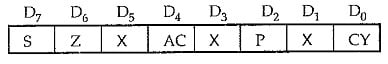
S-Sign flag : After the execution of arithmetic or logical operations, if bit D7 of the result is 1, the sign flag is set. In a given byte if D7 is 1, the number will be viewed as negative number. If D7 is 0, the number will be considered as positive number.
Z-Zero flag : The zero flag sets if the result of operation in ALU is zero and flag resets if result is non zero. The zero flag is also set if a certain register content becomes zero following an increment or decrement operation of that register.
AC-Auxiliary Carry flag : This flag is set if there is an overflow out of bit 3 i.e. carry from lower nibble to higher nibble (D3 bit to D4 bit). This flag is used for BCD operations and it is not available for the programmer.
P-Parity flag: Parity is defined by the number of ones present in the accumulator. After an arithmetic or logical operation, if the result has an even number of ones, i.e. even parity, the flag is set. If the parity is odd, the flag is reset.
CY-Carry flag: This flag is set if there is an overflow out of bit 7. The carry flag also serves as a borrow flag for subtraction. In both the examples shown below, the carry flag is set.
c) Instruction Register: In a typical processor operation, the processor first fetches the opcode of instruction from memory (i.e. it places an address on the address bus and memory responds by placing the data stored at the specified address on the data bus). The CPU stores this opcode in a register called the instruction register. This opcode is further sent to the instruction decoder to select one of the 256 alternatives.
16-Bit Registers:
a) Program counter (PC) : Program is a sequence of instructions. As mentioned earlier, microprocessor fetches these instructions from the memory and executes them The program counter is a special purpose register which, at a given time, stores the address of the next instruction to be fetched. Program Counter acts as a pointer to the next instruction.
How processor increments program counter depends on the nature of the instruction; for one-byte instruction, it increments program counter by one, for two-byte instruction it increments program counter by two and for three-byte .instruction it increments program counter by three such that program counter always points to the address of the next instruction.
In case of JUMP and CALL instructions, address followed by JUMP and CALL instructions is placed in the program counter. The processor then fetches the next instruction from the new address specified by JUMP or CALL instruction. In conditional JUMP and conditional CALL instructions, if the condition is not satisfied, the processor increments program counter by three so that it points the instruction followed by conditional JUMP or CALL instruction; otherwise processor fetches the next instruction from the new address specified by JUMP or CALL instruction.
b) Stack Pointer (SP) : The stack is a reserved area of the memory in the RAM where temporary information may be stored. A 16-bit stack pointer is used to hold the address of the most recent stack entry.
Arithmetic Logic Unit (ALU):
The 8085’s ALU performs arithmetic and logical functions on eight bit variables. The arithmetic unit performs bitwise fundamental arithmetic operations such as addition and subtraction. The logic unit performs logical operations such as complement, AND, OR and EX-OR, as well as rotate and clear. The ALU also looks after the branching decisions.
Instruction Decoder:
As mentioned earlier, the processor first fetches the opcode of instruction from memory and stores this opcode in the instruction register. It is then sent to the instruction decoder. The instruction decoder decodes it and accordingly gives the timing and control signals which control the register, the data buffers, ALU, and external peripheral signals depending on the nature of the instruction.
The 8085 Microprocessor Architecture executes seven different types of machine cycles. It gives the information about which machine cycle is currently executing in the encoded form on the S0, S1 and IO/M lines. This task is done by machine cycle encoder.
Address Buffer:
This is an 8-bit unidirectional buffer. It is used to drive an external high order address bus (A15 – A8). It is also used to tri-state the high order address bus under certain conditions such as reset, hold, halt, and when address lines are not in use.
Address/Data Buffer:
This is an 8-bit bi-directional buffer. It is used to drive multiplexed address/data bus, i.e. low order address bus (A7 – A0) and data bus (D7 – D0). It is also used to tri-state the multiplexed address/data bus under certain conditions such as reset, hold, halt and when the bus is not in use.
The address and data buffers are used to drive external address and data buses respectively. Due to these buffers the address and data buses can be tri-stated when they are not in use.
Incrementer/Decrementer Address Latch:
This 16-bit register is used to increment or decrement the contents of program counter or stack pointer as a part of execution of instructions related to them.
Interrupt Control:
The processor fetches, decodes, and executes instructions in a sequence. Sometimes it is necessary to have processor the automatically execute one of a collection of special routines whenever special condition exists within a program or the microcomputer system. The most important thing is that, after the execution of the special routine, the program control must be transferred to the program which processor was executing before the occurrence of the special condition. The occurrence of this special condition is referred to as an interrupt. The interrupt control block has five interrupt inputs RST 5.5, RST 6.5, RST 7.5, TRAP, and INTR and one acknowledge signal INTA.
Serial I/O Control:
In situations like data transmission over long distances and communication with cassette tapes or a CRT terminal, it is necessary to transmit data bit by bit to reduce the cost of cabling. In serial communication, one bit is transferred at a time over a single line. The 8085’s serial I/O control provides two lines, SOD and SID for serial communication. The serial output data (SOD) line is used to send data serially and serial input data (SID) line is used to receive data serially.
Timing and Control Circuitry:
The control circuitry in the processor 8085 Microprocessor Architecture is responsible for all the operations. The control circuitry and hence the operations in 8085 Microprocessor Architecture are synchronized with the help of clock signal. Along with the control of fetching and decoding operations and generating appropriate signals for instruction execution, control circuitry also generates signals required to interface external devices to the processor, 8085 Microprocessor Architecture.
References
- A.P.Godse, D.A.Godse, Microprocessors & Microcontrollers, India, Technical Publications