Table of Contents
IMPATT Diode
IMPATT diode is abbreviated as an impact-ionization avalanche transit-time diode. It is an active solid-state device that operates by a reverse bias adequate to cause avalanche breakdown. This is a high-power diode and a very powerful microwave source that is used in high-frequency electronics and microwave devices. They may be operated at frequencies up to about 350 GHz when manufactured with silicon.
The IMPATT diode exhibits a dynamic negative resistance that is required for microwave oscillation and amplification applications. This is due to the following two reasons:
Impact Ionization avalanche effect: This causes the carrier current to lag behind the ac voltage by 90 degrees.
Transit time effect: This causes a further time delay and causes the external current to lag behind the ac voltage by a further 90 degrees.
The summation of delay involved in generating avalanche current multiplication along with delay due to transit time through drift space provides the necessary 180° phase difference between the applied voltage and the resulting current in an IMPATT diode.
These devices can be classified as follows:
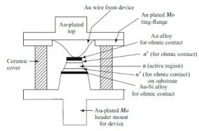
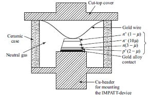
Single drift devices: Devices such as P+NN+, N+PP+, P+NIN+, and N+PIP+ come under this category. Consider the P+NN+ device. In this device, when the P+N junction is reverse biased, it causes an avalanche breakdown. This causes the P+ region to inject electrons into the NN+ region. These electrons move with a saturated velocity. However, the holes injected from the NN+ region do not drift. Hence, these are called single drift devices.
Double drift devices: The example of a double drift device is P+PNN+. In this device, when the PN junction is biased near an avalanche breakdown, electrons drift along the NN+ region and holes drift along the PP+ region. Hence, they are called double drift devices.
Principle of Operation of IMPATT Diode
To understand the operation of an IMPATT diode, here we consider the N+PIP+ diode. Let Vb be the reverse bias breakdown voltage that is applied to the IMPATT device. Assume that a sinusoidal waveform V1 sinω t is superimposed on Vdc, resulting in a total device voltage V (t) = (Vdc + V1 sinω t) as shown in the figure below.

Working of IMPATT diode
Initially, the device contains a few thermally generated free electrons. When V(t) > Vb breakdown occurs at the N+P junction, these electrons gain energy from the applied voltage and knock off electrons in the valence band to the conduction band. As a result, a new electron-hole pair is created. An electron-hole pair generated because of such impact ionization is called a secondary electron-hole pair.
These secondary electrons again pick up sufficient energy and generate more secondary electron-hole pairs. Therefore, as long as V(t) > Vb, the number of carriers increases exponentially, even beyond the voltage maximum irrespective of the magnitude of V(t).
This is because of the sufficient number of secondary electron-hole pairs presence. This exponential increase continues until the sine wave crosses zero and then drops exponentially until the sine wave reaches its negative peak. This avalanche current (generated holes) is injected into the I-region and drifts toward the P+ region with saturated velocity along the depletion region. The electrons move toward the positive terminal. In this way, this current will have a one-quarter period (T/4) delay or a 90° phase shift with regard to the applied signal voltage.
To achieve the desired 180° phase shift between input voltage and external current, additional T/4 delay is essential. This is made available by the hole drift along the depletion region. It is the property of semiconductor materials that the drift velocity tends to be constant at high field strengths. Since the holes move at the constant velocity vd, the device length may be chosen to provide the necessary delay for a 180° phase shift between the device voltage and current, which is given by
l=v_{d}\frac{T}{4}
Equivalent Circuit:
The IMPATT diode equivalent circuit is as shown in the figure below. It is composed of two parts that are the avalanche and drift regions, and a loss resistance (Rs). One part of the equivalent circuit is the avalanche region it consists of a resonant circuit, with an avalanche inductance (La) and a capacitance (Ca). The avalanche capacitance is given by:
C_{a}=\frac{\epsilon_{s}S}{w_{a}}
where,
- wa is the width of the avalanche region,
- εs = permittivity of the dielectric, and
- A is the area.
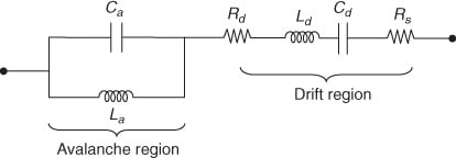
The IMPATT diode exhibits negative resistance for frequencies higher than the avalanche resonant frequency ( fa ), and is given by
f_{a}=l/\sqrt{L_{a}C_{a}}
Characteristics of IMPATT Diode
- IMPATT diode operates in reverse bias. It exhibits a negative resistance region due to the impact of avalanche and transit time effects.
- The phase difference between voltage and current is 180°. Here 90° phase delay is due to the avalanche effect, and the remaining 90° is due to transit time effect.
- It is a narrow-band amplifier that provides output power in the millimeter-wave frequency range.
- At low frequencies, their power output is inversely proportional to frequency. At high frequencies, their power output is inversely proportional to the square of the frequency.
- They are often used in the design of oscillators and amplifiers when the high output power is required. They provide higher output power than Gunn diodes.
- IMPATT diodes are manufactured in Si, GaAs, and InP. They can be operated up to 350 GHz when manufactured in Si.
- These diodes are of low cost, reliable, and compact. They are moderately efficient milliwatt power sources.
- These are noisier than Gunn diodes. Therefore, they are rarely used for local oscillators in receivers.
Performance characteristics
- Theoretical, η = 30% (< 30% in practice) and 15% for Si, 23% for GaAs
- Frequency: 1 to 300 GHz
- Maximum output power for a single diode: 5W in X band to 6.5 W at 30 GHz
- Several diodes combined: 40 W in X band
- Pulsed powers = 4 kW
Disadvantages of IMPATT diode
- In terms of noise figure an IMPATT diode is not good as in comparison with the TWT amplifier or Gunn diode oscillator or klystron tube. Because the avalanche is a high noise process, so the IMPATT is very noisy diode, the value of noise figure is 30 dB.
- In IMPATT diode matching is difficult because of the low value of their negative resistance.
- It is sensitive to operational conditions.
- It has large electronic reactance, which can cause detuning or burn out the device if proper care is not taken.
Applications of IMPATT Diode
- IMPATT diodes are used as microwave oscillators in microwave generators, in modulated output oscillators.
- They are used in microwave links, continuous-wave radars, and electronic countermeasures.
- IMPATT diodes are also used as amplification with negative resistance. In police radars, low power transmitters, and intrusion alarm devices are used the high-Q IMPATT diodes. In frequency modulated telecommunication transmitters and continuous wave Doppler radar transmitters are used the low-Q IMPATT diodes.
Related Posts: