Table of Contents
P-N Junction Diode
A P-N junction diode is a combination of two semiconductor materials, one is P-type semiconductor and another is N-type semiconductor. It is also called as simply P-N junction or semiconductor diode.
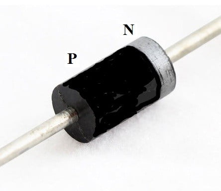
The diode has two terminals, P-type semiconductor is called anode and N-type semiconductor is called cathode. It allows the current in one direction and opposes with high resistance in another direction. it is also called a crystal diode because of its making is in a crystal (Silicon or Germanium) form. Terminals of the diode can be identified by a multimeter.
Circuit Symbol of a diode
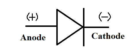
When the diode is used as a circuit element, it is convenient to represent it by a symbol.

Anode and Cathode are two terminals of a diode, where the anode is a P-type semiconductor and the cathode is N-type semiconductor. The anode has a positive voltage whereas the cathode has a negative voltage. The arrowhead symbol the tip points from the P-region towards the N-region. This shows that the direction of conventional current is from the P-region to the N-region which is also the direction of flow of holes.
Properties of a P-N Junction
The p-n junction possesses some interesting properties which have useful applications in modern electronics. A p-doped semiconductor is relatively conductive. The same is true of an n-doped semiconductor, but the junction between them is a nonconductor. This non conductor layer, called the depletion layer zone, occurs because the electrical charge carries in doped n-type and p-type silicon (electrons & holes, respectively) attract and eliminate each other in a process called recombination. By manipulating this non conductive layer, p-n junctions are commonly used as diode: circuit elements that allows a flow of electricity in one direction but not in other (opposite) direction. This property is explained in terms of the forward-bias and revers-bias effects, where the term bias refers to an application of electric voltage to the p-n junction.
V-I characteristics of P-N Junction Diode or Practical Diode
If the diode is used as a circuit element in an electrical circuit, there may be a requirement to know how it responds or behaves in an electric circuit. This type of information may be obtained by a curve known as Volt-Ampere (V-I) characteristics of a practical diode.
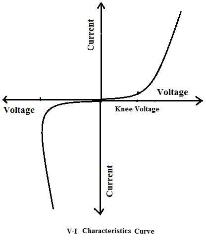
The V-I characteristics of a P-N junction diode is simply a curve or graph between the voltage applied across its terminals and the current that flows through the diode due to this applied voltage. The entire V-I characteristics may be divided into two parts namely:
- Forward characteristics
- Reverse characteristics
Forward Characteristic:
The circuit arrangement is shown in the figure which is used to obtain forward characteristics of a diode. The diode in the circuit is in forward bias state because the battery Vf is pushing the current in the arrowhead.

When the diode is connected with a battery or power source, the P-type semiconductor or anode is connected to a positive terminal and the N-type semiconductor or cathode is connected to the negative terminal of the battery. This configuration of the diode is known as a forward biasing of a diode.
In this basing or configuration diode work like as a short circuit or closed switch. Its forward resistance is very low in the range of ohms. It means the current is easily flow in forward biasing of a diode.
V-I characteristics curve in forward bais
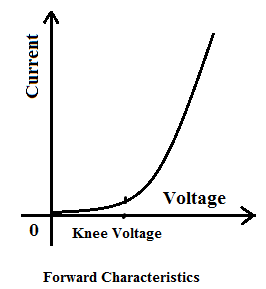
In the V-I characteristics, the voltage across the diode is increased gradually and the corresponding increase in the current. In the forward characteristic curve, the diode current is very small up to a fixed point.
The applied voltage is cross to the barrier potential than the diode current increase rapidly and diode conducts heavily. This barrier voltage at which the current starts increasing is called the knee voltage. The value of knee voltage for silicon diode is 0.7 V and for germanium diode 0.3 V.
In this configuration, the majority charge carriers are holes or positive charge and minority charge carriers are electrons or negative charge.
Reverse Characteristic:
V-I characteristics curve in reverse bais
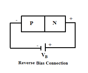
Now in reverse bias configuration, the diode is connected with a battery or power source, the P-type semiconductor or anode is connected to the negative terminal and the N-type semiconductor or cathode is connected to the positive terminal of the battery.
This configuration of a diode is known as a reverse biasing of the diode. In this basing or configuration diode work like as an open circuit or open switch. Its reverse bias resistance is high in the range of megaohms (MΩ). It means a very less current or no current will pass from the junction of the diode.

In the V-I characteristics, the voltage across the diode is negative so a very low current will flow which is nearer about zero. The value of the negative voltage is increased up to a certain level, the amount of current will not be increased. The current is flowing in reverse bias is called as reverse current and is due to minority charge carries.
The value of reverse current is typically less than 1µA and may be as low as 1nA for silicon and the reverse current may exceed 10µA in case of germanium.
Diode Current Equation
The diode current equation, relating the voltage V and current I for the forward and reverse bias regions, can be given by

Here, I = Diode Current
I_{0}= Diode reverse saturation current at room temperature
V = external voltage applied to the diode
η = a constant 1 for germanium and 2 for silicon
It is 1 for germanium and 2 for silicon.
V_{T}=\frac{kT}{q}Where, k = Boltzmann’s constant = 1.38066 x 10⁻²³ J/Kelvin
q = Electronic Charge = 1.6 x 10⁻¹⁹ Coulomb
T = Diode junction temperature in (oK)
Important terms of P-N Junction Diode
Breakdown voltage
In the case of reverse voltage, a small amount of reverse current will flow through P-N junction. After that, when increasing the reverse voltage, it will reach a point at which the junction breaks down with an unexpected increment in the reverse current. Breakdown voltage is defined as “it is a reverse voltage at which P-N junction breaks down with unexpected increment in reverse voltage”.
Knee Voltage
In forward biasing of P-N junction a very small amount of current will pass from the junction until the forward voltage crosses the value of junction barrier potential i.e. 0.3 V for Germanium and 0.7 V for Silicon. The forward voltage, at which the current pass the P-N junction starts very quickly, is called knee voltage or the cut in voltage.
Maximum Forward Current
It is the highest forward current at which a P-N junction will pass current without any damage or problem in the junction. If the forward current will cross this rated value of current, the junction will get crushed because of overheating.
Pear Inverse Voltage
It is the maximum reverse voltage at which the P-N junction will function properly without any damage in the junction. If the reverse voltage will cross the rated value of peak inverse voltage (PIV), the junction may get crushed because of overheating.
Maximum Power Rating
It is the maximum power, which can be dissipated from the junction without any damage or problem in the junction.
Difference between Silicon and Germanium Diodes
| S.No. | Parameter | Silicon Diode | Germanium Diode |
| 1 | Material used | Silicon | Germanium |
| 2 | Cut-in voltage | 0.6 V | 0.2 V |
| 3 | Reverse saturation current | In nanoamp | In microamp |
| 4 | Effect of temperature | Less | More |
| 5 | Breakdown voltage | Higher | Lower |
| 6 | Application | Rectifiers, clippers, clampers, etc | Low voltage Low temperature application |
Applications of Diode
Half-wave Rectifier
In half-wave rectification, the circuit conducts current only during the positive half-cycles of the input a.c. supply. The negative half-cycles of a.c. supply is suppressed i.e. during negative half-cycles, no current is conducted and hence no voltage appears across the load. Therefore, current always flows in one direction (i.e. d.c.) through the load though after every half-cycle.

Full-wave rectifier
In a full-wave rectifier circuit two diodes are used, together with a transfer whose secondary winding is split equally in two and has a center tapped connection. Each diode conducts in turn when its anode terminal is positive with respect to the center point.

Bridge Rectifier
Another type of circuit that produced full-wave rectification is that of the Bridge Rectifier. This type of single phase rectifier uses 4 individual rectifying diodes connected in a “bridged” configuration to produce the desired output but does not required a spacial center taped transformer, thereby reducing its size and cost. The single secondary winding is connected to one side of the diode bridge network and the load to the other side.

