Table of Contents
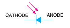
Zener Diode
The Zener diode is a normal PN junction diode. But it is different from PN junction on the basis of doping and also on working principle. When Zener Diode is in forward biasing it behaves just like a normal PN junction diode, but when it is in reverse biasing, it shows different characteristics as compared to the PN junction diode.

The diode, when reverse biased, allows reverse saturation current through it and the saturation current is constant with respect to the applied voltage and depends on the temperature. It doubles for every degree rise in temperature. This is true until a voltage is applied. But as the reverse voltage to the diode increases, this breaks and the current in the diode increases tremendously at a particular voltage. This increase in current is due to either Zener breakdown or Avalanche multiplication in the diode when reverse biased. This feature of the diode, called a breakdown, finds large applications. It acts as a voltage regulator. A voltage regulator is a device that maintains the output voltage constant irrespective of the load or load current. The diodes that are manufactured to be specifically operated in this breakdown region are referred to as Zener or Avalanche or breakdown diodes.
Zener diode V-I characteristics curve
The V-I characteristics curve of the Zener diode is as shown in the figure below. In the reverse bias, the current is constant until a voltage is reached and at this voltage, referred to as Zener voltage, the current multiplies to a very large extent. This region of operation is known as the breakdown region. The diode is said to be in the breakdown region when the current in the diode is more than the threshold current Izk. The current in the diode is limited to the maximum value that can be handled by the diode, specified by the manufacturer.

Avalanche multiplication
When the reverse voltage to the diode is increased to a large extent, two phenomena of breakdown occur. They include Avalanche Multiplication and Zener Breakdown. In Avalanche Multiplication, at the high applied electric fields, the covalent bonds are broken by the virtue of collision of high-speed electrons with the crystalline structure of the material. The intrinsic electrons available in the material get the required acceleration from the applied electric field. When these high-speed electrons strike the covalent bond, the kinetic energy is converted to potential energy and if the potential energy imparted to the bond is sufficient to break the covalent bond, an electron hole-pair is released from the bond. These newly generated electrons gain acceleration by the electric field already available in the diode and thus move with very high velocity to strike and release a new pair of electron and hole.
The process continues and a large number of electron-hole pairs are generated which will drift towards the respective electrodes crossing the junction and get absorbed. This formulates very large currents at the applied reverse voltage. Thus, the current is only due to intrinsic charge carriers crossing the junction below a cutoff voltage, which is the reverse saturation current. But when the voltage applied is such that the electric field is sufficient to impart required energy to break the covalent bond by virtue of collision of high-speed electrons, current in the diode increases sharply. Such a phenomenon of current multiplication is called Avalanche Multiplication.
Zener breakdown
In addition to the above-discussed phenomenon, one more process of increasing the current in the breakdown is possible. This is a Zener breakdown. When the applied voltage is sufficient to establish an electric field that can break the covalent bond, new electron-hole pairs are generated. In this process, no collision of the electrons with the bonds is encountered, but the electric field is itself sufficient to pull out an electron into the conduction band. Thus, a free electron and a hole in the valence band are created for each bond broken. At a given applied field, a large number of bonds are broken and thus a large number of charge carriers are produced. These charge carriers are accelerated and travel down to cross the junction to constitute current in the breakdown region.
Avalanche multiplication or Zener Breakdown can cause the current to breakdown when the diode is reverse biased. Whatever may be the phenomenon occurring in the diode, the diode is referred to as Zener diode. Depending upon the applied voltage and doping levels, either of the phenomena is initiated first. When the current multiplication is initiated, it multiplies and there is no distinction between the two ongoing processes.
The doping levels of the diode determine which process is initiated first. When the doping levels are high such that the electric field is of the order of 2×10⁷ V/m, Zener Breakdown occurs and this is possible up to breakdown voltages of 6V. When the doping is light, avalanche multiplication is initiated and this is possible with diodes having breakdown voltages above 6 V. Diodes can be fabricated with different breakdown voltage right from few volts to several hundred volts. The power handling capacity of such Zener diodes can be of the order of 50 W.
Zener Diode Circuits
In the figure below Vi is the input voltage and V0 is the output voltage. VZ is the Zener diode voltage drop. I is the current from the source and IZ is the current through the Zener diode. IL is the load current.

As long as (Vi – I.Rs) < VZ; the output voltage V0 will be V0 = (Vi – I.Rs), since the Zener diode does not conduct and V0 = (Vi – IL.Rs). Also, IZ = 0 during the non-conduction of the Zener diode.
In Zener diode regulators, when the voltage across the Zener diode is more than or equal to VZ; V0 will be clamped at VZ and V0 = VZ. As the load current increases, it is as though Zener supplies the extra current by reducing its own current. When IL is maximum IZ is minimum and when IL is minimum IZ is maximum. However, IZ minimum is necessary for the Zener diode to enter the regulation mode. The current from the supply source I is the sum of the currents IZ and IL.
I=I_{Z}+I_{L},
I_{Z}=I-I_{L},
I_{L}=I-I_{Z}The value of the resistance RS can be calculated as follows:
R_{S}=\frac{(V_{i}-V_{Z})}{(I_{L}+I_{Z})}=\frac{(V_{i}-V_{Z})}{(I_{L}+0.2I_{L})}=\frac{(V_{i}-V_{Z})}{1.2I_{Z}}With normal operating currents of the Zener diode; IZ is chosen as equal to 0.2.ILoad.
Power PZ dissipated in the Zener diode can be calculated as follows:
P_{Z}=I_{Z}.V_{Z}=\left [ \left ( \frac{(V_{i}-V_{Z})}{R_{S}} \right )-I_{L} \right ]V_{Z}A Zener diode must be selected with a larger power rating than the power dissipation rating PZ that is calculated from the above equation so that the maximum power dissipation and the temperature ratings of the device are not exceeded.
Applications of Zener Diode
- Constant voltage regulation
- Surge protection
- Clamping and clipping voltages
- Voltage reference in precision equipment such as regulated power supply circuits
- Switching operation
- For meter protection.
Advantages
Smaller size, cheaper and has a long life and rugged. It provides good regulation over a wider range of currents.
Drawbacks
- Power loss associated with As for light and heavy load current and poorer efficiency.
- The output voltage depends upon the breakdown voltage of the Zener diode.